The C64 I/O Expander
��������������������
Legal
This document is Copyright � Per Olofsson (E-mail: MagerValp@Goth.Org) but
may be spread freely as long as no changes are made to this document or the
illustrations that are distributed with it.
Archive Contents
IOexpander.txt This document
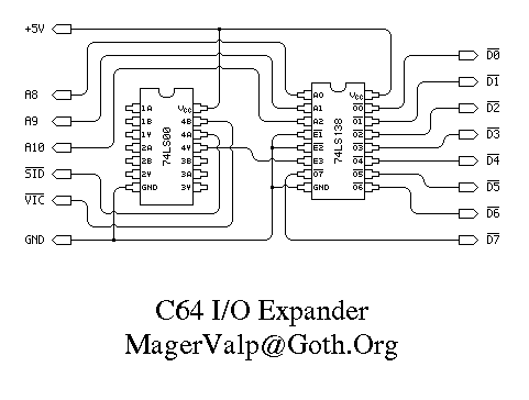
IOexpander.gif The project schematics in B/W
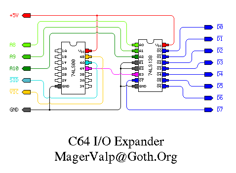
IOexpanderColour.gif The project schematics in colour
Introduction
In the C64 I/O space (D000-DFFF) there are several unused areas below D800
that are filled with mirror images of the VIC and SID registers. By adding
a bit of logic to the address decoding done by the PLA it's possible to
utilize the address space more efficiently. The modification requires basic
soldering skills and a bit of soldering on the C64 motherboard. Please note
that this will void your warranty :)
Parts list
1 74LS00 Quad 2-input NAND gate
1 74LS138 3-line to 8-line decoder/demultiplexer
sockets, wire and a peice of veroboard
Schematic
+5V <==--------------------+-----------------------.
.-----------------|---------. |
| .---------------|-------. | | .--------==> /D0
| | .-------------|-----. | | __ __ | |
| | | __ __ | | | | | `-' | | | .------==> /D1
A8 <==--' | | | `-' | | | | `-[|0 16|]-' | |
| | [|0 14|]-' | `---[| |]---' | .----==> /D2
A9 <==----' | [| |]---. `-----[| |]-----' |
| [| |]-. | .---[|74LS138|]-------' .--==> /D3
A10 <==------' [|74LS00 |]-|-|--. +---[| |]---------'
[| |] | | `--|---[| |]------------==> /D4
/SID <==----. [| |] | | | .-[| |]------.
| .-[|6 7|] | | +-|-[|7 8|]----. `-----==> /D5
/VIC <==--. | | |_______| | | | | |_______| |
| `-|-------------' | | | `-------==> /D6
`---|---------------' | |
GND <==------+---------------------' `------------------------==> /D7
I have included two GIF images
Description
+5 V and ground can be taken from just about anywhere on the motherboard.
The SID chip select signal is on pin 8 and the VIC chip select signal is on
pin 10. A8, A9 and A10 can be taken from the character ROM on pins 23, 22
and 19.
Out of the decoder you get eight active low chip select signals. The /D0
and /D4 signals should be soldered to the /CS pins on the VIC and the SID,
respectively. If everything worked out OK you now have six free 256 byte
areas in the I/O space.